KIT - Karlsruhe Institute of Technology image/svg+xml
Institute for Photon Science and Synchrotron Radiation
  • skip navigation
  • Home
  • Legals
  • Privacy Policy
  • Sitemap
  • KIT
    • IPS Home
    • Research
      • Research
      Research
      • Materials and Processes for Energy Technologies
      • Nanostructures, Materials & Devices for Information Technologies
      • Materials & Processes for Transport Technologies
      • Imaging Technologies for Life Science and Materials Research
      • Collaboration & Innovation
    • Methods & Facilities
      • Methods & Facilities
      Methods & Facilities
      • IMAGING Cluster
      • SCATTERING Cluster
      • SPECTROSCOPY Cluster
    • News
    • Publications
    • People
    • KIT Light Source
    • Contact
    • Jobs
    • Startpage
    • Home
    • Legals
    • Privacy Policy
    • Sitemap
    Institute for Photon Science and Synchrotron Radiation


    • Startpage
    • Methods & Facilities
    • SCATTERING Cluster


    • Startseite
      • IPS Home
      • Research
      • Methods & Facilities
      • News
      • Publications
      • People
      • KIT Light Source
      • Contact
      • Jobs
    • Methods & Facilities
      • IMAGING Cluster
      • SCATTERING Cluster
      • SPECTROSCOPY Cluster
    • SCATTERING Cluster
    • UHV Lab
    • Cluster
    • Methods
    • Chambers
    • UHV-Chemistry Lab
    • Contact
    • Publications

    UHV Lab

    The IPS UHV (ultra-high vacuum) Analysis lab is a facility for in-situ growth studies combining a modular and extendable UHV cluster system for complementary surface analytics with several UHV growth chambers for in situ X-ray experiments during thin film and nanostructure formation.


    The UHV cluster is a large ultra-high vacuum transfer system offering several docking stations for portable and stationary growth chambers. Samples with a maximum size of 25 mm can be inserted directly via three loadlocks. The central analysis and surface preparation chambers are accessible from all growth chambers.


    Situated close to the IPS beamlines and to a dedicated chemistry lab for sample preparation, the UHV Analysis lab allows for studying various nanosystems, optimizing the use of the beamlines, and ensures a fast feedback between complementary measurements and X-ray experiments.


    Samples can be prepared by Argon sputtering (limited to a surface area of 10x10 mm2) and annealing. They can be analyzed by standard surface characterization methods such as:


    • reflection high energy electron diffraction (RHEED),
    • low-energy electron diffraction (LEED),
    • Auger electron spectroscopy (AES),
    • X-ray photoelectron spectroscopy (XPS),
    • UHV atomic force microscopy (AFM),
    • UHV scanning tunneling microscopy (STM).


    The UHV cluster is an extendable facility which can be expanded to meet the demands of future experiments. 


    UHV cluster comprising several deposition and surface analysis chambers.

    Cluster

    Functional units of UHV Cluster 

    UHV-Cluster Image courtesy of CreaTec Fischer & Co. GmbH, AFM image courtesy of Omicron Nano Technology GmbH

    Methods

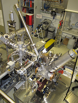
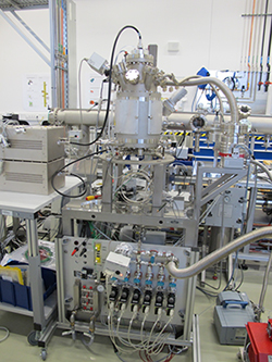
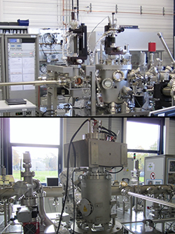
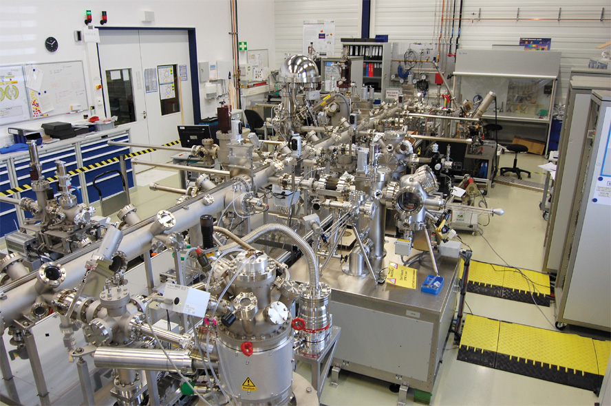
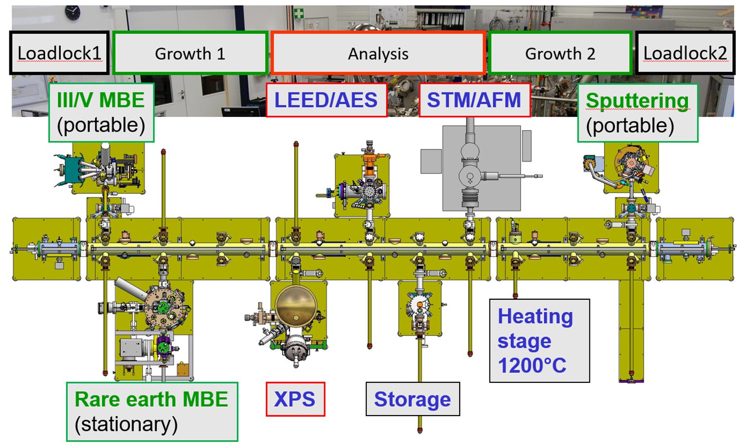
    In the UHV analysis lab, samples can be analyzed by several standard surface characterization methods including spectroscopical methods (XPS and AES), diffraction methods (LEED and RHEED) and scanning microscopy (AFM and STM). Here, an overview over the methods is given. As an example, measurements of a gold single crystal are shown.

    XPS - X-ray Photoelectron Spectroscopy

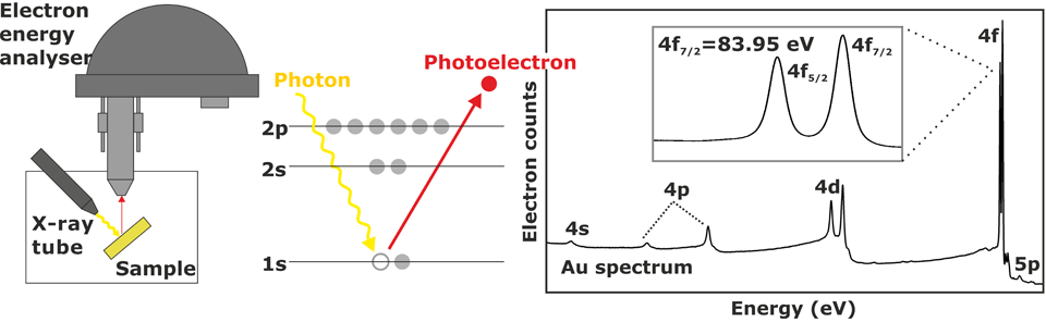
    X-ray photoelectron spectroscopy gives information about the chemical composition of a sample within the topmost 2 nm. The sample is illuminated by soft X-rays. Photoelectrons are emitted, giving information about the binding energies of the atoms.

    AES - Auger Electron Spectroscopy

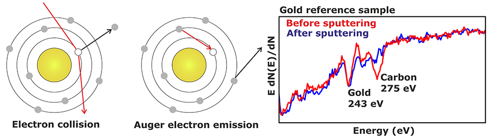
    Auger electron spectroscopy is another method to get information about chemical composition. Auger electrons are emitted from atoms, giving information about binding energies. One application of the method is to check a sample for surface contaminations, e.g. after contact with air.

    LEED - Low Energy Electron Diffraction

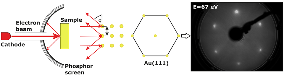
    Low energy electron diffraction gives information about the atomic ordering of a material, by bombarding it with a beam of low energy electrons. The pattern of the structure, created by the diffracted electrons; is shown on a screen.


    RHEED - Reflection High Energy Electron Diffraction

    Reflection high energy electron diffraction is another method to examine the crystalline structure of the surface. Streaks indicate a smooth surface.

    AFM - Atomic Force Microscopy

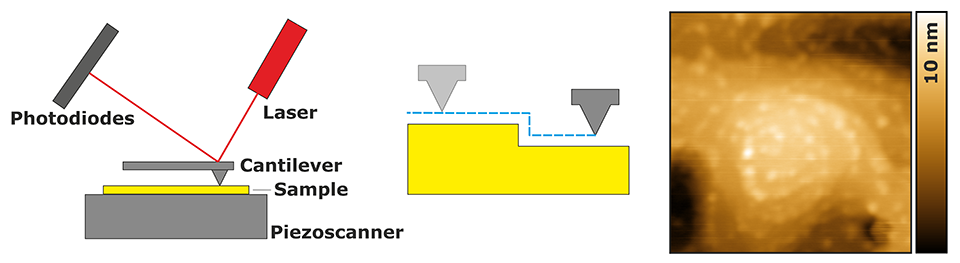
    An atomic force microscope is a high-resolution scanning microscope which gives information about the surface morphology of a material on the atomic scale. The measured signal is the bending of a cantilever which is related to the force between a tip and the sample.

    STM - Scanning Tunnel Microscopy

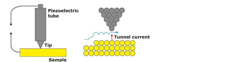
    Another method for imaging surfaces is the scanning tunnel microscopy. The measured signal is a tunnel current between a tip and the sample.


    Chambers

    Portable in situ MBE chamber

    Portable chamber for in situ sputter deposition


    Rare-earth MBE chamber


    Real-time in situ X-ray investigations of dynamic processes during epitaxial growth and annealing of III-V semiconductor nanostructures (e.g. GaAsNW, InGaAsQD).

    In situ X-ray experiments (XRD, XRR, EXAFS) during reactive and non-reactive sputter deposition of thin films.

    Investigation of the interplay between the structure, morphology, magnetism and lattice dynamics in rare earth based epitaxial nanostructures.

    Materials:
    InGaAs  
    Materials:
    transition metal nitrides and carbides, metals, silicides          
    Materials:
    rare earth metals, silicides and oxides  

    Special features:

    RHEED

    Special features:

    modular chamber geometry, large angular range for XRD, RF and DC magnetron sputtering

    Special features:

    several high temperature evaporation sources, Tubo-e cell for oxides, in situ RHEED and MOKE measurements

    Contact: Julian Jakob

    Research Project:

    „III-V Semiconductor Nanostructures“

    Contact: Bärbel Krause

    Research Project: „Sputter deposition“

    Contact: Svetoslav Stankov 

    Research Group: „Nanodynamics“

    Reference UHV chamber:

    Slobodskyy et al., Rev. Sci. Instr. 83 (2012), 105112-105117 

    Reference UHV chamber:

    Krause et al., J. Synchr. Rad.19 (2012), 216-222 

    Reference UHV chamber:

    S. Ibrahimkutty et al., J. Sync. Rad. 22 (2015) 1 


    more information...      

    more information...       

    more information...     

    UHV-Chemistry Lab

    The UHV- Chemistry Lab, which is directly connected to the UHV analysis laboratory, is optimized for the needs of thin film preparation such as sample surface preparation by etching, thin film deposition from solution, and cleaning of UHV components.
    4
    Storage and disposal containers
    Ultrasonic bath
    STM tip eatching divice

    The chemistry lab is equipped with two fume hoods (standard & for strong acids). Storage space and disposal containers for acids, bases, and solvents are available.
     

    Typical tasks:

    • Cleaning samples, holder and UHV-components in the ultrasonic bath
    • Chemical cleaning and etching of samples and components
    • Preparation of AFM and STM tips
    • HF etching of Si Substrates


    Contact:

    Lab Responsible: Dr. Bärbel Krause
    Chemical Technical Contact: Annette Weißhardt

    Contact(s)
    Name Function E-mail
    Krause, Bärbel Scientist baerbel krause ∂does-not-exist.kit edu

    Publications from the UHV Lab.


    Solid-state reactions at the metal-semiconductor interface
    Krause, B.; Abadias, G.; Babonneau, D.; Michel, A.; Resta, A.; Coati, A.; Garreau, Y.; Vlad, A.; Plech, A.; Wochner, P.; Baumbach, T.
    2024. Highlights de SOLEIL 2023, 50–51, Synchrotron Soleil
    Understanding the role of supported Rh atoms and clusters during hydroformylation and CO hydrogenation reactions with in situ / operando XAS and DRIFT spectroscopy
    Sarma, B. B.; Neukum, D.; Doronkin, D. E.; Lakshmi Nilayam, A. R.; Baumgarten, L.; Krause, B.; Grunwaldt, J.-D.
    2024. Chemical Science, 15 (31), 12369–12379. doi:10.1039/D4SC02907K
    Lattice dynamics of β − FeSi₂ nanorods
    Kalt, J.; Sternik, M.; Sergeev, I.; Mikolasek, M.; Bessas, D.; Göttlicher, J.; Krause, B.; Vitova, T.; Steininger, R.; Sikora, O.; Jochym, P. T.; Leupold, O.; Wille, H.-C.; Chumakov, A. I.; Piekarz, P.; Parlinski, K.; Baumbach, T.; Stankov, S.
    2022. Physical Review B, 106 (20), Article no: 205411. doi:10.1103/PhysRevB.106.205411
    In Situ Monitoring of MBE Growth of a Single Self-Catalyzed GaAs Nanowire by X-ray Diffraction
    Mostafavi Kashani, S. M.; Dubrovskii, V. G.; Baumbach, T.; Pietsch, U.
    2021. The journal of physical chemistry <Washington, DC> / C, 125 (41), 22724–22732. doi:10.1021/acs.jpcc.1c04255
    Chiral phonons in the honeycomb sublattice of layered CoSn-like compounds
    Ptok, A.; Kobiałka, A.; Sternik, M.; Łażewski, J.; Jochym, P. T.; Oleś, A. M.; Stankov, S.; Piekarz, P.
    2021. Physical Review B, 104 (5), Art.-Nr.: 054305. doi:10.1103/PhysRevB.104.054305
    Chemical Structure of a Carbon-Rich Layer at the Wet-Chemical Processed CuZnSn(S,Se)/Mo Interface
    Hauschild, D.; Wachs, S. J.; Kogler, W.; Seitz, L.; Carter, J.; Schnabel, T.; Krause, B.; Blum, M.; Yang, W.; Ahlswede, E.; Heske, C.; Weinhardt, L.
    2021. IEEE Journal of Photovoltaics, 11 (3), 658–663. doi:10.1109/JPHOTOV.2021.3059423
    Liveschaltung zum Dünnschichtwachstum – Ein Echtzeit‐Einblick in das Wechselspiel zwischen Struktur und Eigenspannung während der Sputterdeposition
    Krause, B.; Abadias, G.
    2020. Vakuum in Forschung und Praxis, 32 (6), 26–31. doi:10.1002/vipr.202000748
    Lattice dynamics of endotaxial silicide nanowires
    Kalt, J.; Sternik, M.; Krause, B.; Sergueev, I.; Mikolasek, M.; Merkel, D.; Bessas, D.; Sikora, O.; Vitova, T.; Göttlicher, J.; Steininger, R.; Jochym, P. T.; Ptok, A.; Leupold, O.; Wille, H.-C.; Chumakov, A. I.; Piekarz, P.; Parlinski, K.; Baumbach, T.; Stankov, S.
    2020. Physical review / B, 102 (19), Art.-Nr.: 195414. doi:10.1103/PhysRevB.102.195414
    Quantitative analysis of in situ time-resolved RHEED during growth of self-catalysed GaAs nanowires. PhD dissertation
    Jakob, J. B.
    2020, August 26. Karlsruher Institut für Technologie (KIT). doi:10.5445/IR/1000122870
    Lattice dynamics and polarization-dependent phonon damping in α-phase FeSi2 nanostructures
    Kalt, J.; Sternik, M.; Krause, B.; Sergueev, I.; Mikolasek, M.; Bessas, D.; Sikora, O.; Vitova, T.; Göttlicher, J.; Steininger, R.; Jochym, P. T.; Ptok, A.; Leupold, O.; Wille, H.-C.; Chumakov, A. I.; Piekarz, P.; Parlinski, K.; Baumbach, T.; Stankov, S.
    2020. Physical review / B, 101 (16), Art.-Nr.: 165406. doi:10.1103/PhysRevB.101.165406
    Interfacial Silicide Formation and Stress Evolution during Sputter Deposition of Ultrathin Pd Layers on a-Si
    Krause, B.; Abadias, G.; Furgeaud, C.; Michel, A.; Resta, A.; Coati, A.; Garreau, Y.; Vlad, A.; Hauschild, D.; Baumbach, T.
    2019. ACS applied materials & interfaces, 11 (42), 39315–39323. doi:10.1021/acsami.9b11492
    Piezoelectric 3-D Fibrous Poly(3-hydroxybutyrate)-Based Scaffolds Ultrasound-Mineralized with Calcium Carbonate for Bone Tissue Engineering: Inorganic Phase Formation, Osteoblast Cell Adhesion, and Proliferation
    Chernozem, R. V.; Surmeneva, M. A.; Shkarina, S. N.; Loza, K.; Epple, M.; Ulbricht, M.; Cecilia, A.; Krause, B.; Baumbach, T.; Abalymov, A. A.; Parakhonskiy, B. V.; Skirtach, A. G.; Surmenev, R. A.
    2019. ACS applied materials & interfaces, 11 (21), 19522–19533. doi:10.1021/acsami.9b04936
    Structural and Thermal Characterisation of Nanofilms by Time-Resolved X-ray Scattering
    Plech, A.; Krause, B.; Baumbach, T.; Zakharova, M.; Eon, S.; Girmen, C.; Buth, G.; Bracht, H.
    2019. Nanomaterials, 9 (4), Article: 501. doi:10.3390/nano9040501
    Low-temperature argon and ammonia plasma treatment of poly-3-hydroxybutyrate films: Surface topography and chemistry changes affect fibroblast cells in vitro
    Surmenev, R. A.; Chernozem, R. V.; Syromotina, D. S.; Oehr, C.; Baumbach, T.; Krause, B.; Boyandin, A. N.; Dvoinina, L. M.; Volova, T. G.; Surmeneva, M. A.
    2019. European polymer journal, 112, 137–145. doi:10.1016/j.eurpolymj.2018.12.040
    Functionalization of titania nanotubes with electrophoretically deposited silver and calcium phosphate nanoparticles: Structure, composition and antibacterial assay
    Chernozem, R. V.; Surmeneva, M. A.; Krause, B.; Baumbach, T.; Ignatov, V. P.; Prymak, O.; Loza, K.; Epple, M.; Ennen-Roth, F.; Wittmar, A.; Ulbricht, M.; Chudinova, E. A.; Rijavec, T.; Lapanje, A.; Surmenev, R. A.
    2019. Materials science and engineering / C, 97, 420–430. doi:10.1016/j.msec.2018.12.045
    Plasmonic Hybrid Biocomposite as an Effective Substrate for Detection of Biomolecules by Surface-Enhanced Raman Spectroscopy
    Chernozem, R. V.; Surmeneva, M. A.; Atkin, V.; Krause, B.; Baumbach, T.; Parakhonskiy, B. V.; Khalenkow, D.; Skirtach, A. G.; Surmenev, R. A.
    2018. Russian physics journal, 61 (7), 1288–1293. doi:10.1007/s11182-018-1531-2
    Multifunctional Scaffolds with Improved Antimicrobial Properties and Osteogenicity Based on Piezoelectric Electrospun Fibers Decorated with Bioactive Composite Microcapsules
    Timin, A. S.; Muslimov, A. R.; Zyuzin, M. V.; Peltek, O. O.; Karpov, T. E.; Sergeev, I. S.; Dotsenko, A. I.; Goncharenko, A. A.; Yolshin, N. D.; Sinelnik, A.; Krause, B.; Baumbach, T.; Surmeneva, M. A.; Chernozem, R. V.; Sukhorukov, G. B.; Surmenev, R. A.
    2018. ACS applied materials & interfaces, 10 (41), 34849–34868. doi:10.1021/acsami.8b09810
    In situ and real-time monitoring of structure formation during non-reactive sputter deposition of lanthanum and reactive sputter deposition of lanthanum nitride
    Krause, B.; Kuznetsov, D. S.; Yakshin, A. E.; Ibrahimkutty, S.; Baumbach, T.; Bijkerk, F.
    2018. Journal of applied crystallography, 51 (4), 1013–1020. doi:10.1107/S1600576718007367
    Hydrotreatment of Fast Pyrolysis Bio-oil Fractions Over Nickel-Based Catalyst
    Schmitt, C. C.; Raffelt, K.; Zimina, A.; Krause, B.; Otto, T.; Rapp, M.; Grunwaldt, J.-D.; Dahmen, N.
    2018. Topics in catalysis, 61 (15-17), 1769–1782. doi:10.1007/s11244-018-1009-z
    Theoretical and experimental study of the gradient properties and the resulting local crystalline structure and orientation in magnetron-sputtered CrAlN coatings with lateral composition and thickness gradient
    Krause, B.; Stube, M.; Zimin, A.; Steininger, R.; Trappen, M.; Ulrich, S.; Kashani, S. M. M.; Baumbach, T.
    2017. Journal of applied crystallography, 50, 1000–1010. doi:10.1107/S1600576717006513
    Hybrid biocomposites based on titania nanotubes and a hydroxyapatite coating deposited by RF-magnetron sputtering : Surface topography, structure, and mechanical properties
    Chernozem, R. V.; Surmeneva, M. A.; Krause, B.; Baumbach, T.; Ignatov, V. P.; Tyurin, A. I.; Loza, K.; Epple, M.; Surmenev, R. A.
    2017. Applied surface science, 426, 229–237. doi:10.1016/j.apsusc.2017.07.199
    RF magnetron sputtering of a hydroxyapatite target: A comparison study on polytetrafluorethylene and titanium substrates
    Surmenev, R. A.; Surmeneva, M. A.; Grubova, I. Y.; Chernozem, R. V.; Krause, B.; Baumbach, T.; Loza, K.; Epple, M.
    2017. Applied surface science, 414, 335–344. doi:10.1016/j.apsusc.2017.04.090
    The effect of NaCl on room-temperature-processed indium oxide nanoparticle thin films for printed electronics
    Häming, M.; Baby, T. T.; Garlapati, S. K.; Krause, B.; Hahn, H.; Dasgupta, S.; Weinhardt, L.; Heske, C.
    2017. Applied surface science, 396, 912–919. doi:10.1016/j.apsusc.2016.11.060
    Direct Observation of the Thickness-Induced Crystallization and Stress Build-Up during Sputter-Deposition of Nanoscale Silicide Films
    Krause, B.; Abadias, G.; Michel, A.; Wochner, P.; Ibrahimkutty, S.; Baumbach, T.
    2016. ACS applied materials & interfaces, 8 (50), 34888–34895. doi:10.1021/acsami.6b12413
    Angle-resolved X-ray reflectivity measurements during off-normal sputter deposition of VN
    Krause, B.; Kaufholz, M.; Kotapati, S.; Schneider, R.; Müller, E.; Gerthsen, D.; Wochner, P.; Baumbach, T.
    2015. Surface and coatings technology, 277, 52–57. doi:10.1016/j.surfcoat.2015.07.030
    Monitoring the thin film formation during sputter deposition of Vanadium Carbide
    Kaufholz, M.; Krause, B.; Kotapati, S.; Köhl, M.; Mantilla, M. F.; Stüber, M.; Ulrich, S.; Schneider, R.; Gerthsen, D.; Baumbach, T.
    2015. Journal of synchrotron radiation, 22 (1), 76–85. doi:10.1107/S1600577514024412
    Temperature dependent epitaxial growth regimes of europium on the oxygen-induced c(6×2) reconstructed (110)Nb surface
    Bauder, O.; Seiler, A.; Ibrahimkutty, S.; Merkel, D. G.; Krause, B.; Rüffer, R.; Baumbach, T.; Stankov, S.
    2014. Journal of crystal growth, 400, 61–66. doi:10.1016/j.jcrysgro.2014.04.012
    Influence of a low-temperature capping on the crystalline structure and morphology of InGaN quantum dot structures
    Krause, B.; Miljevic, B.; Aschenbrenner, T.; Piskorska-Hommel, E.; Tessare, C.; Barchuk, M.; Buth, G.; Donfeu Tchana, R.; Figge, S.; Gutowski, J.; Hänschke, D.; Kalden, J.; Laurus, T.; Lazarev, S.; Magalhaes-Paniago, R.; Sebald, K.; Wolska, A.; Hommel, D.; Falta, J.; Holy, V.; Baumbach, T.
    2014. Journal of alloys and compounds, 585, 572–579. doi:10.1016/j.jallcom.2013.09.005
    Composition-dependent structure of polycrystalline magnetron-sputtered V-Al-C-N hard coatings studied by XRD, XPS, XANES and EXAFS
    Krause, B.; Darma, S.; Kaufholz, M.; Mangold, S.; Doyle, S.; Ulrich, S.; Leiste, H.; Stüber, M.; Baumbach, T.
    2013. Journal of applied crystallography, 46 (4), 1064–1075. doi:10.1107/S0021889813014477
    Modular deposition chamber for in situ X-ray experiments during RF and DC magnetron sputtering
    Krause, B.; Darma, S.; Kaufholz, M.; Gräfe, H. H.; Ulrich, S.; Mantilla, M.; Weigel, R.; Rembold, S.; Baumbach, T.
    2012. Journal of Synchrotron Radiation, 19, 216–222. doi:10.1107/S0909049511052320
    last change: 2024-12-13
    KIT – The Research University in the Helmholtz Association
    • Home
    • Legals
    • Privacy Policy
    • Sitemap
    • KIT