
Real-time characterisation of thin-film microstructure using synchrotron X-ray reflectivity
-
The application areas of thin films are extremely diverse, ranging from several micrometre thick protective layers to sub-nanometre active layers in optoelectronic devices. Independent of the application, a common problem is the stress-induced degradation of the layers: tensile stress promotes crack formation, while compressive stress may induce delamination of the film. Even if the device is not visibly damaged, application-relevant properties such as band gap or optical reflectance may already have been affected.
Stress build-up already occurs during deposition of the thin films. However, it is extremely difficult to disentangle its microstructural origins. In polycrystalline thin films for example, possible sources of stress such as interface formation, island coalescence, and grain boundary formation are often related, and stress relaxation mechanisms such as texture, phase and morphology changes occur in competition.
To identify the microstructural origins of the stress evolution, we have developed a unique experimental approach in collaboration with the University of Poitiers, combining real-time curvature measurements (giving information about the stress evolution) with synchrotron x-ray reflectivity and diffraction (giving information about the microstructure evolution) during sputter deposition of thin films[1].
We have demonstrated the feasibility of this experimental approach in the case of metal/silicon interface formation. Two examples were considered: the Mo/Si interface [1] which is relevant for optical applications such as mirrors for telescopes and lithography optics, and the Pd/Si interface [2] which is of interest for silicon-based semiconductor devices, e.g. as precursor state for silicide interconnects.
Even for the comparatively simple metal/silicon interface, our experiments reveal a complex relationship between stress evolution and interface formation, which is significantly influenced by the chemical reactivity. Understanding the structure formation and the resulting stress evolution, however, offers the possibility to use real-time stress measurements as a simple, low-cost, and extremely precise solution for controlling the growth process.
|
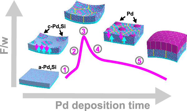
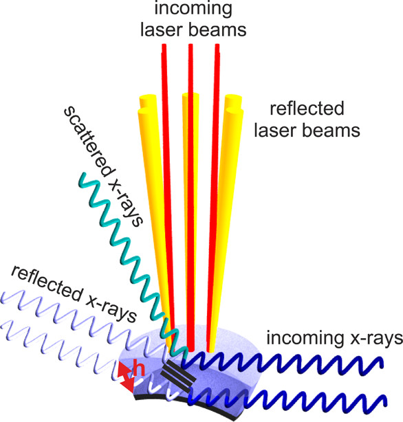
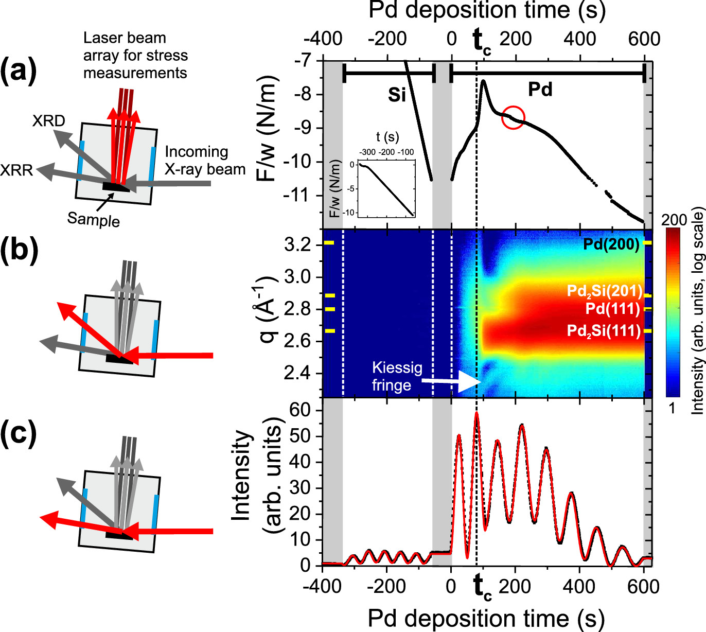
Measurement geometry (left column) and simultaneous real-time measurements (right column) during deposition of Pd on a-Si: (a) Stress measurements, (b) diffraction data, and (c) X-ray reflectivity measurements (black) and fit curve (red). The deposition periods of a-Si and Pd as well as the observed Bragg peaks of Pd and Pd2Si (yellow bars) are indicated. tc indicates the onset of crystallization. |
|
Publications
[1] Krause, B.; Abadias, G.; Michel, A.; Wochner, P.; Ibrahimkutty, S.; Baumbach, T., Direct Observation of the Thickness-Induced Crystallization and Stress Build-Up during Sputter-Deposition of Nanoscale Silicide Films, ACS applied materials & interfaces, 8 (50) 2016, 34888–34895, doi:10.1021/acsami.6b12413
[2] Krause, B.; Abadias, G.; Furgeaud, C.; Michel, A.; Resta, A.; Coati, A.; Garreau, Y.; Vlad, A.; Hauschild, D.; Baumbach, T., Interfacial Silicide Formation and Stress Evolution during Sputter Deposition of Ultrathin Pd Layers on a-Si, ACS applied materials & interfaces, 11 (42) 2019, 39315–39323. doi:10.1021/acsami.9b11492