
Nanostructures, Materials & Devices for Information Technologies
The fabrication, processing and functionalization of materials based on nanostructures involves multiscale processes which often prohibit conventional characterization approaches. The penetration depth of X-rays, together with the brilliance of synchrotron radiation make X-ray scattering and diffraction techniques highly attractive for characterizing these materials. Complementary to locally-resolving electron microscopy, these X-ray techniques give access to macroscopically representative statistical structure correlation properties at micro-, nano-, and atomic length scales. Using coherent diffraction imaging techniques even individual nano-objects can be investigated.
Current research within the general area of Nanostructures, Materials & Devices for Information Technologies includes:
|
|
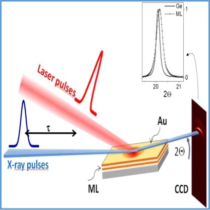
Ultrafast Laser-based Nanomaterials Research |
|
|
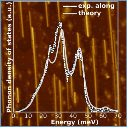
Lattice dynamics, electronic and magnetic properties of thin-films |
|
|
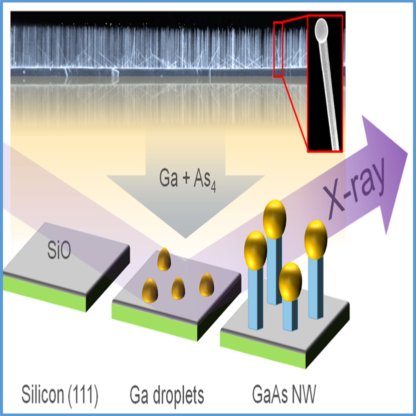
III-V-based nanostructures |
|
|
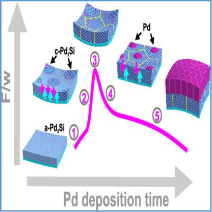
Functional polycrystalline thin-film materials Polycrystalline sputtered coatings are omnipresent in modern functional materials: they are found as anti-reflection coatings on eyeglass lenses, active layers in sensor chips, or hard coatings to extend the life of tools and medical implants. In situ X-ray measurements provide direct insight into the formation of the microstructure during sputtering, and contribute to growth models and an understanding of the interplay between microstructure and macroscopic material function. |
|
|
Correlation of growth parameters and structure of epitaxial oxide thin films • the role of growth parameters on defect formation in dielectric oxide materials |
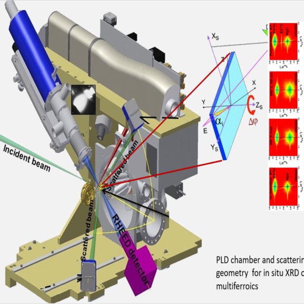
These activities build on the X-ray SCATTERING Cluster at IPS, with its state-of- the-art NANO beamline and experimental station equipped with heavy duty diffractometers for single crystal and powder diffraction, grazing incidence surface and interface scattering techniques, and at other synchrotron facilities such as ESRF, PETRA III, SOLEIL, and SLS.
Dedicated in situ instrumentation, such as Pulsed Laser Deposition (PLD), Metal-Organic Vapor Phase Epitaxy (MOVPE), Molecular Beam Epitaxy (MBE), and sputtering, directly allow X-ray scattering experiments during thin-film and nanostructure formation. These studies are complemented by extensive surface and thin-film analysis facilities such as Reflection High-Energy Electron Diffraction (RHEED), Low-Energy Electron Diffraction (LEED), Auger Electron Spectroscopy (AES), XPS, as well as Atomic-Force Microscopy (AFM) and Scanning-Tunneling Microscopy (STM) at the IPS UHV-analytical lab.