
Fabrication and characterisation of functional thin-film materials
Polycrystalline sputtered coatings are essential for everyday life today: they are found as anti-reflection coatings on eyeglass lenses, active layers in sensor chips, or hard coatings to extend the life of tools and medical implants. Depending on the application of the coating, different material properties are required which are directly related to its microstructure. However, the microstructure produced during the film formation is still only predictable to a limited extent. In situ X-ray measurements (i.e. X-ray measurements during film growth) can help by providing direct insight into the formation of the microstructure during the sputtering process.
The main aim of our research is to advance the understanding of structure formation in sputter deposited thin films and nanostructures. This includes several tasks:
- Development of synchrotron-based methods for monitoring the interface formation, crystal growth, and phase formation during deposition
- Application of these methods to various material systems and structures
- Derivation of growth models
- Investigation of the interplay between microstructure and microscopic material properties
- Application of research results: production of specific layers with the desired properties
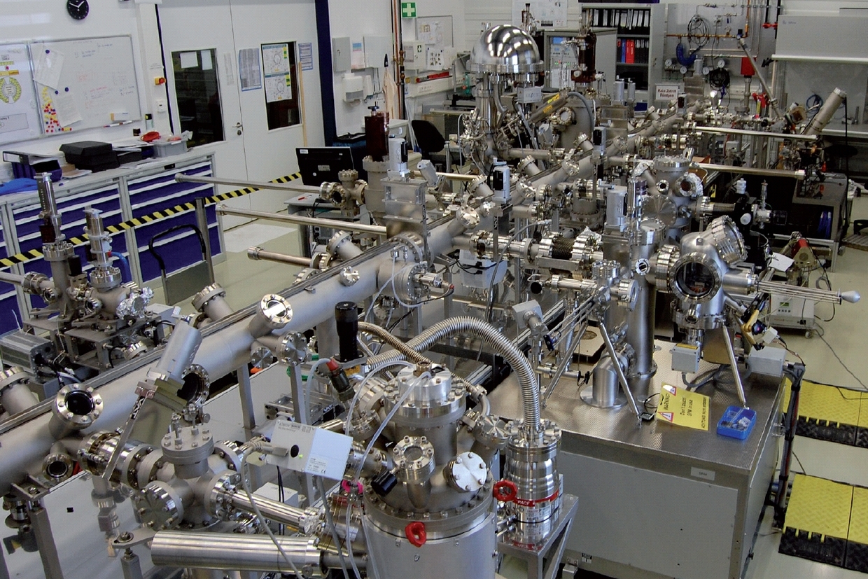
To fabricate and analyse thin-film materials we employ various methods:
- Reactive and non-reactive RF and DC magnetron sputtering
- In situ X-ray scattering methods (X-ray diffraction, pole figure measurements, X-ray reflectivity) during thin film growth
- Spectroscopic methods (XPS, EXAFS, XANES)
- Microscopy (AFM, TEM, optical microscopy) and electron diffraction (RHEED) methods
For model systems such as:
- Hard coating materials based on nitrides and carbides of transition metals (e.g. CrAlN, VN)
- Silicides and Germanides (e.g. MoSi, WSi)
Contact