KIT - Karlsruhe Institute of Technology image/svg+xml
Institute for Photon Science and Synchrotron Radiation
  • skip navigation
  • Home
  • Legals
  • Privacy Policy
  • Sitemap
  • KIT
    • IPS Home
    • Research
      • Research
      Research
      • Materials and Processes for Energy Technologies
      • Nanostructures, Materials & Devices for Information Technologies
      • Materials & Processes for Transport Technologies
      • Imaging Technologies for Life Science and Materials Research
      • Cooperations & 3rd-party Projects
    • Methods & Facilities
      • Methods & Facilities
      Methods & Facilities
      • IMAGING Cluster
      • SCATTERING Cluster
      • SPECTROSCOPY Cluster
    • News
    • Publications
    • People
    • Commercial Services
    • KIT Light Source
    • Contact
    • Jobs
    • Startpage
    • Home
    • Legals
    • Privacy Policy
    • Sitemap
    Institute for Photon Science and Synchrotron Radiation


    • Startpage
    • Methods & Facilities
    • SCATTERING Cluster


    • Startseite
      • IPS Home
      • Research
      • Methods & Facilities
      • News
      • Publications
      • People
      • Commercial Services
      • KIT Light Source
      • Contact
      • Jobs
    • Methods & Facilities
      • IMAGING Cluster
      • SCATTERING Cluster
      • SPECTROSCOPY Cluster
    • SCATTERING Cluster
    • NANO
    • Layout & Characteristics
    • Methods
    • Publications
    • Contact

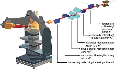
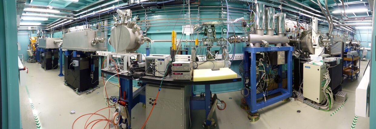
    The NANO Beamline at the KIT Light Source is dedicated to high-resolution X-ray diffraction, surface and interface X-ray scattering investigations. The beamline has been optimized to deliver a monochromatic and highly collimated beam with sufficient flux to investigate structural changes and strain evolution during the growth of epitaxial films and superlattices.


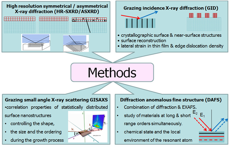
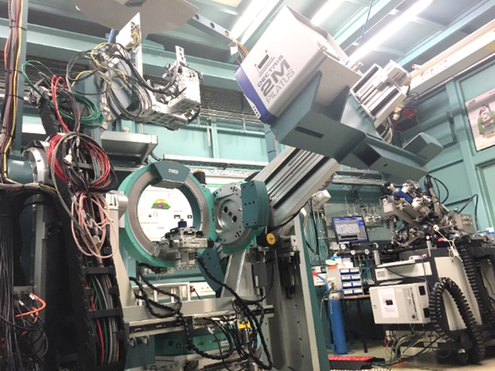
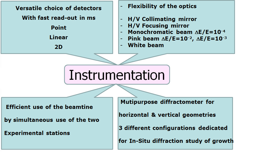
    In order to carry out real time measurements, different types of environmental chambers, e.g., for molecular beam epitaxy, are mounted on the heavy duty diffractometer which supports up to 500 kg. The diffractometer allows rotation of the sample and the environmental parts in all directions in space. With two different detection systems on the diffractometer, it is possible to perform simultaneous measurement such as Grazing Incidence Small Angle X-ray Scattering (GISAXS), to determine the shape, size, position and correlation in nanostructures, and Grazing Incidence Diffraction (GID) to characterize the surface-patterned structure. One of the main uses of the beamline is to study interface properties like roughness and correlation even for weakly scattering materials such as organic semiconductors.


    A further focus of our research is the real time monitoring of nanoparticles and nanostructures. 


    Beamline Layout

    NANO is designed for high-resolution x-ray diffraction, surface and interface X-ray scattering investigations.


    ​


    Methods and applications


    The main scientific applications of the NANO beamine are:


    • Thin films and multilayers
    • Surfaces and interfaces
    • Nanostructures (2D and 3D) and nanomaterials
    • Real-Time monitoring of growing epitaxial thin films, superlattices and nanoparticles
    • Characterization of shape, size, position and their correlations in nanostructures
    • Defect analysis in crystal structures
    • In-situ and ex-situ growth studies of crystals, organic and inorganic films


    Publications


    1. Effect of pulse laser frequency on PLD growth of LuFeO3 explained by kinetic simulations of in-situ diffracted intensities
      Gabriel, V.; Kocán, P.; Bauer, S.; Nergis, B.; Rodrigues, A.; Horák, L.; Jin, X.; Schneider, R.; Baumbach, T.; Holý, V.
      2022. Scientific Reports, 12 (1), Artkl.Nr.:5647. doi:10.1038/s41598-022-09414-3
    2. Time-Resolved Morphology and Kinetic Studies of Pulsed Laser Deposition-Grown Pt Layers on Sapphire at Different Growth Temperatures by in Situ Grazing Incidence Small-Angle X-ray Scattering
      Bauer, S.; Rodrigues, A.; Horák, L.; Nergis, B.; Jin, X.; Schneider, R.; Gröger, R.; Baumbach, T.; Holý, V.
      2021. Langmuir, 37 (2), 734–749. doi:10.1021/acs.langmuir.0c02952
    3. In situ grazing-incidence x-ray scattering study of pulsed-laser deposition of Pt layers
      Holý, V.; Bauer, S.; Rodrigues, A.; Horák, L.; Jin, X.; Schneider, R.; Baumbach, T.
      2020. Physical review / B, 102 (12), Article: 125435. doi:10.1103/PhysRevB.102.125435
    4. Combined In Situ XRD and Ex Situ TEM Studies of Thin Ba0.5Sr0.5TiO3 Films Grown by PLD on MgO
      Bauer, S.; Rodrigues, A.; Jin, X.; Schneider, R.; Müller, E.; Gerthsen, D.; Baumbach, T.
      2020. Crystal research and technology, 55 (9), Art. Nr.: 1900235. doi:10.1002/crat.201900235
    5. Structure Quality of LuFeO3 Epitaxial Layers Grown by Pulsed-Laser Deposition on Sapphire/Pt
      Bauer, S.; Rodrigues, A.; Horák, L.; Jin, X.; Schneider, R.; Baumbach, T.; Holý, V.
      2020. Materials, 13 (1), Art. Nr.: 61. doi:10.3390/ma13010061
    6. Revealing misfit dislocations in InAsxP1−x-InP core–shell nanowires by x-ray diffraction
      Lazarev, S.; Göransson, D. J. O.; Borgström, M.; Messing, M. E.; Xu, H. Q.; Dzhigaev, D.; Yefanov, O. M.; Bauer, S.; Baumbach, T.; Feidenhans’l, R.; Samuelson, L.; Vartanyants, I. A.
      2019. Nanotechnology, 30 (50), Article: 505703. doi:10.1088/1361-6528/ab40f1
    7. Real time in situ x-ray diffraction study of the crystalline structure modification of Ba0.5Sr0.5TiO₃ during the post-annealing
      Bauer, S.; Rodrigues, A.; Baumbach, T.
      2018. Scientific reports, 8 (1), Article No. 11969. doi:10.1038/s41598-018-30392-y
    8. Effect of post-annealing on the chemical state and crystalline structure of PLD Ba0.5Sr0.5TiO3 films analyzed by combined synchrotron X-ray diffraction and X-ray photoelectron spectroscopy
      Rodrigues, A.; Bauer, S.; Baumbach, T.
      2018. Ceramics international, 44 (13), 16017–16024. doi:10.1016/j.ceramint.2018.06.038
    9. Optimizing structural and mechanical properties of cryogel scaffolds for use in prostate cancer cell culturing
      Cecilia, A.; Baecker, A.; Rack, A.; Hamann, E.; Kamp, T. van de; Gruhl, F. J.; Hofmann, R.; Moosmann, J.; Hahn, S.; Kashef, J.; Bauer, S.; Faragó, T.; Helfen, L.; Baumbach, T.
      2017. Materials science and engineering / C, 71, 465–472. doi:10.1016/j.msec.2016.10.038
    10. Microwave synthesis of high-quality and uniform 4 nm ZnFe₂O₄ nanocrystals for application in energy storage and nanomagnetics
      Suchomski, C.; Breitung, B.; Witte, R.; Knapp, M.; Bauer, S.; Baumbach, T.; Reitz, C.; Brezesinski, T.
      2016. Beilstein journal of nanotechnology, 7, 1350–1360. doi:10.3762/bjnano.7.126
    11. In operando study of the high voltage spinel cathode material LiNi₀̣₅Mn₁̣₅O₄ using two dimensional full-field spectroscopic imaging of Ni and Mn
      Bauer, S.; De Biasi, L.; Glatthaar, S.; Toukam, L.; Geßwein, H.; Baumbach, T.
      2015. Physical chemistry, chemical physics, 17, 16388–16397. doi:10.1039/C5CP02075A
    12. Evolution of polytypism in GaAs nanowires during growth revealed by time-resolved in situ x-ray diffraction
      Schroth, P.; Köhl, M.; Hornung, J.-W.; Dimakis, E.; Somaschini, C.; Geelhaar, L.; Biermanns, A.; Bauer, S.; Lazarev, S.; Pietsch, U.; Baumbach, T.
      2015. Physical review letters, 114, 055504/1–6. doi:10.1103/PhysRevLett.114.055504
    13. Three-dimensional reciprocal space mapping with a two-dimensional detector as a low-latency tool for investigating the influence of growth parameters on defects in semipolar GaN
      Bauer, S.; Lazarev, S.; Bauer, M.; Meisch, T.; Caliebe, M.; Holy, V.; Scholz, F.; Baumbach, T.
      2015. Journal of applied crystallography, 48, 1000–1010. doi:10.1107/S1600576715009085
    14. The power of in situ pulsed laser deposition synchrotron characterization for the detection of domain formation during growth of Ba₀̣₅Sr₀̣₅TiO₃ on MgO
      Bauer, S.; Lazarev, S.; Molinari, A.; Breitenstein, A.; Leufke, P.; Kruk, R.; Hahn, H.; Baumbach, T.
      2014. Journal of Synchrotron Radiation, 21 (2), 386–394. doi:10.1107/S1600577513034358
    15. Three-dimensional reciprocal space mapping of diffuse scattering for the study of stacking faults in semipolar (1122) GaN layers grown from the sidewall of an r-patterned sapphire substrate
      Lazarev, S.; Bauer, S.; Meisch, T.; Bauer, M.; Tischer, I.; Barchuk, M.; Thonke, K.; Holy, V.; Scholz, F.; Baumbach, T.
      2013. Journal of applied crystallography, 46 (5), 1425–1433. doi:10.1107/S0021889813020438
    16. Growth and doping of semipolar GaN grown on patterned sapphire substrates
      Scholz, F.; Meisch, T.; Caliebe, M.; Schörner, S.; Thonke, K.; Kirste, L.; Bauer, S.; Lazarev, S.; Baumbach, T.
      2014. Journal of crystal growth, 405, 97–101. doi:10.1016/j.jcrysgro.2014.08.006
    17. Studies on defect reduction in AlGaN heterostructures by integrating an in-situ SiN interlayer
      Scholz, F.; Forghani, K.; Klein, M.; Klein, O.; Kaiser, U.; Neuschl, B.; Tischer, I.; Feneberg, M.; Thonke, K.; Lazarev, S.; Bauer, S.; Baumbach, T.
      2013. Japanese journal of applied physics, 52 (8S), 08JJ07/1–4. doi:10.7567/JJAP.52.08JJ07
    18. High resolution synchrotron X-ray studies of phase separation phenomena and the scaling law for the threading dislocation densities reduction in high quality AlGaN heterostructure
      Lazarev, S.; Bauer, S.; Forghani, K.; Barchuk, M.; Scholz, F.; Baumbach, T.
      2013. Journal of Crystal Growth, 370, 51–56. doi:10.1016/j.jcrysgro.2012.07.033
    19. Study of threading dislocation density reduction in AlGaN epilayers by Monte Carlo simulation of high-resolution reciprocal-space maps of a two-layer system
      Lazarev, S.; Barchuk, M.; Bauer, S.; Forghani, K.; Holy, V.; Baumbach, T.; Scholz, F.
      2013. Journal of applied crystallography, 46 (Part 1), 120–127. doi:10.1107/S0021889812043051
    20. Simulation of X-ray beamlines with the new ray tracing tool XTrace
      Bauer, S. T.; Bauer, M.; Steininger, R.; Baumbach, T.
      2007. Nuclear instruments & methods in physics research / A, (2007), 582 (1), 90–92. doi:10.1016/j.nima.2007.08.068
    Contact
    name function e-mail
    Bauer, Sondes Deputy Head of Department, Beamline Scientist sondes bauer ∂does-not-exist.kit edu
    last change: 2021-09-29
    KIT – The Research University in the Helmholtz Association
    • Home
    • Legals
    • Privacy Policy
    • Sitemap
    • KIT