
Intelligent Real-time MAnipulation of metal nanostructure growth (IRMA)
IRMA seeks to develop effective, non-invasive strategies for manipulating morphology and opto-electronic properties of vapor-deposited Ag nanostructures, such as 3D nanoparticles and ultra-thin continuous layers. The approach relies on selective deployment of additives (i.e., gaseous species and solute metals) to target key nanostructure formation stages, whereby complex dynamic synthesis processes will be studied in real-time by leveraging the strengths of lab-scale in situ probes and synchrotron X-ray tools.
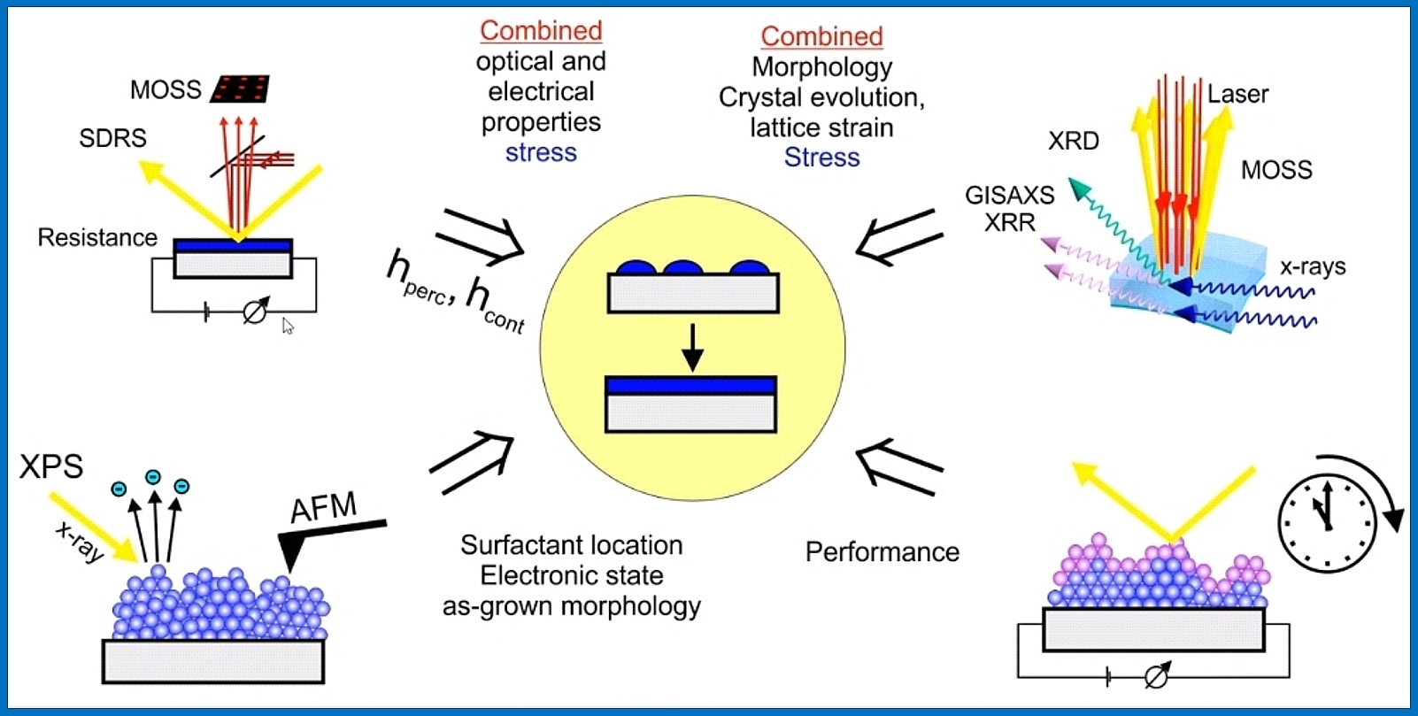
Wafer curvature (stress) measurements combined with X-ray diffraction, X-ray reflectivity and small-angle X-ray scattering will provide insights into the interplay among crystal formation, morphological evolution, and stress development, which will be used to benchmark data from real-time optical and electrical probes. On a grander scale, the fundamental knowledge generated by the IRMA project paves the way toward intelligent in-line control of industrial nanostructure synthesis processes.
Project Partners
IPS, KIT
Université de Poitiers, Frankreich
Synchrotron SOLEIL, Frankreich
Funding
The project is funded by the Deutsche Forschungsgemeinschaft (DFG) under the project number 491224986, and by the Agence Nationale de la Recherche (ANR) under the project number ANR-21-CE09-0041-01 (link: https://anr.fr/Projet-ANR-21-CE09-0041)


Publications
- Zhao, G. et al. Nitrogen-Mediated Growth of Silver Nanocrystals to Form UltraThin, High-Purity Silver-Film Electrodes with Broad band Transparency for Solar Cells. ACS Appl. Mater. Interfaces 10, 40901-40910 (2018). https://doi.org/10.1021/acsami.8b13377
- Yun, J. et al. An unexpected surfactant role of immiscible nitrogen in the structural development of silver nanoparticles: An experimental and numerical investigation. Nanoscale 12, 1749–1758 (2020). https://doi.org/10.1039/C9NR08076G
- Zhang, J. et al. Phenomenological Model of the Growth of Ultrasmooth Silver Thin Films Deposited with a Germanium Nucleation Layer. Langmuir 31, 7852–7859 (2015). https://doi.org/10.1021/acs.langmuir.5b01244
- Jamnig, A. et al. 3D-to-2D Morphology Manipulation of Sputter-Deposited Nanoscale Silver Films on Weakly Interacting Substrates via Selective Nitrogen Deployment for Multifunctional Metal Contacts. ACS Appl. Nano Mater. 3, 4728–4738 (2020). https://doi.org/10.1021/acsanm.0c00736
- Simonot, L., Chabanais, F., Rousselet, S., Camelio, S. & Babonneau, D. Evolution of plasmonic nanostructures under ultra-low-energy ion bombardment. Appl. Surf. Sci. 544, 148672 (2021). https://doi.org/10.1016/j.apsusc.2020.148672
- Colin, J. et al. In situ and real-time nanoscale monitoring of ultra-thin metal film growth using optical and electrical diagnostic tools. Nanomaterials 10, 2225 (2020). https://doi.org/10.3390/nano10112225
- Krause, B. et al. Direct Observation of the Thickness-Induced Crystallization and Stress Build-Up during Sputter-Deposition of Nanoscale Silicide Films. ACS Appl. Mater. Interfaces 8, 34888–34895 (2016). https://doi.org/10.1021/acsami.6b12413
- B. Krause et al., ACS Applied Mater. Interfaces 2023, 15, 1268–1128. https://pubs.acs.org/doi/10.1021/acsami.2c20600