
A New Crystal Experience
- Date: 2017
-
A New Crystal Experience
A new, very generally applicable imaging approach provides not only three-dimensional information about complex arrangements of dislocations inside monocrystals, but also allows us to investigate precisely the behavior and role of all the individual defects during plastic deformation process. Based on this methodology, we are able to shed new light on the mechanisms involved in the thermally induced plastic deformation of silicon wafers, the understanding and prediction of which is crucial for semiconductor processing in the context of present and future scientific and industrial applications.
Nowadays, it is well known that the nucleation, motion, and interaction of dislocations, i.e. of crystalline line defects, dominate the plastic behavior of any crystal material. Since their first direct observation in the 1950s, electron microscopy has provided invaluable insight into the nature of dislocations, recently also in three dimensions. The extremely high resolution inherent to this technique, however, comes at the price of a highly invasive preparation of very small sample volumes, which hinders the direct study of bulk properties and precludes the investigation of many application relevant questions typically involving large crystals like wafers. With our novel correlative imaging approach, we aim on closing this gap, providing comprehensive three-dimensional access to the ‘mesoscopic’ length scale between a few hundred nanometers and several millimeters.
In short, our correlative approach combines data from 2D and 3D X-ray diffraction imaging, as well as from visible light microscopy. In this way, not only the 3D paths of the individual dislocations can be precisely determined even within complex arrangements, but also the complete distribution of the so-called Burgers vectors (the direction and amount of the deformation carried by a single dislocation) is accessible. Moreover, we can study the relation between these bulk properties and many surface features like causative mechanical damage. The methodology is fully non-destructive even for large samples with considerable lateral extension like wafers, and thus it suits novel in situ studies with application relevance for scientific and industrial applications. It may be applied for the characterization of any monocrystalline material.
Based on this novel approach, we present a study of thermally induced deformation of Si wafers, originating from prior mechanical damage, i.e. emulating typical damage during industrial semiconductor processing. While here the completely new generation of dislocations turns out to play only a minor role, we identify the mobilization and multiplication of pre-existing dislocations as dominating mechanisms. For the first time, we observe undisturbed long-range emission of dislocations from regenerative sources, which is a potential issue for the future manufacturing of further miniaturized microelectronic devices.
Figure 1:
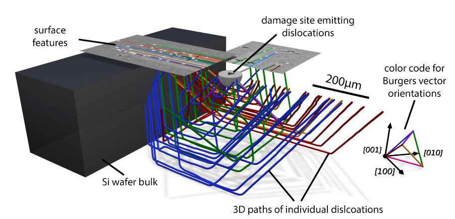
Illustration of a comprehensive picture of dislocations inside a Si wafer, obtained by means of the novel correlative imaging approach.
Figure 2:
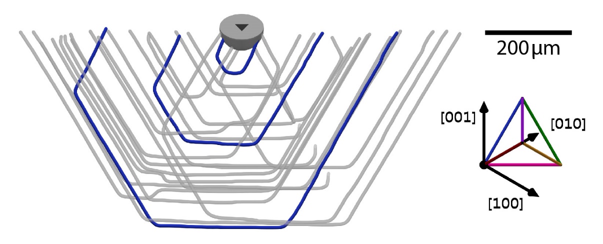
First observation of undisturbed long-distance dislocation emission from a regenerative, Frank-Read-type source (blue) within typical, closely populated (grey) and only 5-10µm thick {111} slip-bands. The associated individual surface steps superpose and thus result in one high step, which is a potential issue for the future manufacturing of further miniaturized microelectronic devices.
The work was supported by the allocation of beam time at the ESRF and partially funded by EU-FP7 Project No. 216382 “SIDAM” and by the German Bundesministerium für Bildung, Forschung und Technologie Grant No. 05K14VFA “STROBOS-CODE.”
Publication:
D. Hänschke, A. Danilewsky, L. Helfen, E. Hamann, and T. Baumbach, „Correlated Three-Dimensional Imaging of Dislocations: Insights into the Onset of Thermal Slip in Semiconductor Wafers”, Phys. Rev. Lett. 119, 215504 (2017).
Further reading:
D. Hänschke, L. Helfen, V. Altapova, A. Danilewsky, and T. Baumbach, „Three-dimensional imaging of dislocations by X-ray diffraction laminography”, Appl. Phys. Lett. 101, 244103 (2012).
A.N. Danilewsky, J. Wittge, A. Cröll, D. Allen, P. McNally, P. Vagovic, T. d. S. Rolo, T. d. S., Z. Li, T. Baumbach, E. Gorostegui-Colinas, J. Garagorri, M. R. Elizalde, M. C. Fossati, D. K. Bowen, B. K. Tanner, “Dislocation dynamics and slip band formation in silicon: In-situ study by X-ray diffraction imaging”, J. Cryst. Growth 318, 1157 (2011).